ECE 252
Week 1
Universal Compute
- Turing Machine: any computable computation can be implemented by some machine
- Universal Turing Machine: A programmable computer is effectively a Universal Turing Machine (minus infinite memory).
- A computer can compute anything that’s possible to compute given enough memory and time.
- Design trade-off: Time, Cost, Power/Energy.
Complexity
- 1st transistor -> Bell Labs, 1st IC -> Jack Kilby(MSEE’50), 1st microprocessor -> Intel
- Moore’s Law: number of transistors on a microchip doubles approximately every two years(24 month). -> Cost halves every two years.
Abstraction
- Use abstraction to manage complexity.
- The ISA lies at the software/hardware boundary.
- Problem Statement –Software Design–> Algorithm –Programming–> Program –Compilation–> ISA –Processor Design–> Microarchitecture –Logic/Circuit Design–> Logic Circuits –Implement&Fabricate–> Devices
Electral Infomation
- Analog: continuous range of values
- Digital: discrete set of values (almost all eletronic device)
- In reality, the voltage levels are actually ranges of voltages.
- Voltage = Current * Resistance
- Any data processed by a digital computer is represented by sequences of 1s and 0s
Week 2
Number representation
- demical-10, Binary-2, Octal-8, Hexademical-16
- least-significant, right most; most-significant, left-most
- $D_{N-1}\cdots D_{1}D_{0}=D_{N-1}*r^{N-1} + \cdots + D_{1}r^1 + D_0r^0$
- Each position represents a power of base; Digital value says how many of that power of base.
- A value is a particular quantity, a number is a way to represent a value. Same “number”, different value.
Base conversion
- Binary <-> Hex: directly substitute a hex digit for a 4-bit binary number.
- Binary <-> Octal: directly substitute a octual digit for a 3-bit binary number.
- Octal <-> Hex: use binary as an intermediate form.
Arithmetic
- Substraction using borrowing: If necessary, bowrrow the base’s value from one position higher
- Multiple by power of base, shifts number to the left. Divide by power of base, shifts numbers to the right.
Signed Numbers
- Signed-Magnitude: The most significant bit is the sign, the remaining bits are the numbers magnitude.
- 2’s Complement representation: positive numbers start with 0, negative numbers start with 1 ($-2^N$).
- Fast Negation: complement each bit and the add 1.
- Addition: works the way it does for unsigned binary number except the carry-out is not meaningful.
- Substraction: add the negation of the value we wish to subtract
- Operand/Result bitwidths match: operands and results must have the same number of bits for the math to work correctly.
Sign Extention
- Extend 2’s complement number: for positive: zero-extension; for negative: one-extension
- Negative 1 in 2’s complement: $-1\cdots1$
- Unsigned number: $[0, 2^n -1]$, signed number: $[-(2^{n-1}-1), 2^{n-1}-1]$, 2’s-complement number: $[-2^{n-1}, 2^{n-1}-1]$
- Overflow: The result cannot be correctly represented in the required number of bits.
- lf adding two negative 2’s-complement numbers overflows, the sign of the result will appear to be non-negative.
- lf the result of adding two positive 2’s-complement numbers appears to be positive, then the operation did not overflow.
- lf adding two unsigned numbers overflows , the result will appear to be
smaller than it should be.
Week 3
Fixed Float
- Radix point: separates the integer portion from the fractional portion of the numebr
- when the format defines a “fixed” position for the radix point within the number’s digits

- Shifting right by $N$ bits is equivalent to dividing by $2^N$
- location of radix is not visible, not encoded in the number, must told. We never know the meaning of a binary number just by looking at it.
Floating Float
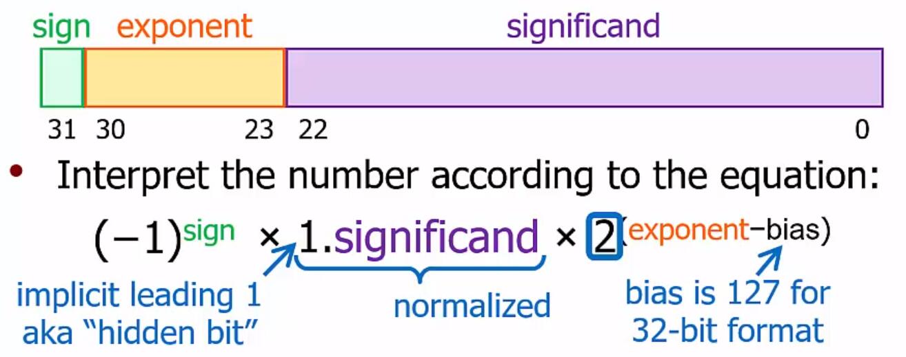
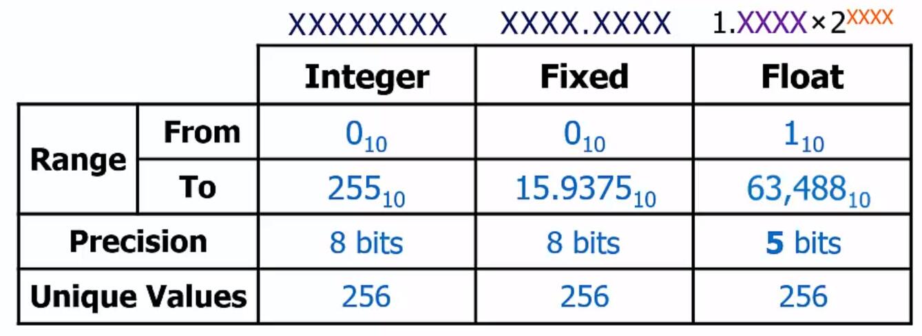
- Precision: number of significant digits. No need to transform 10.
ASCII
- 7 bits to represent 128 different characters.
- UTF-8, 16, 32
Week 4
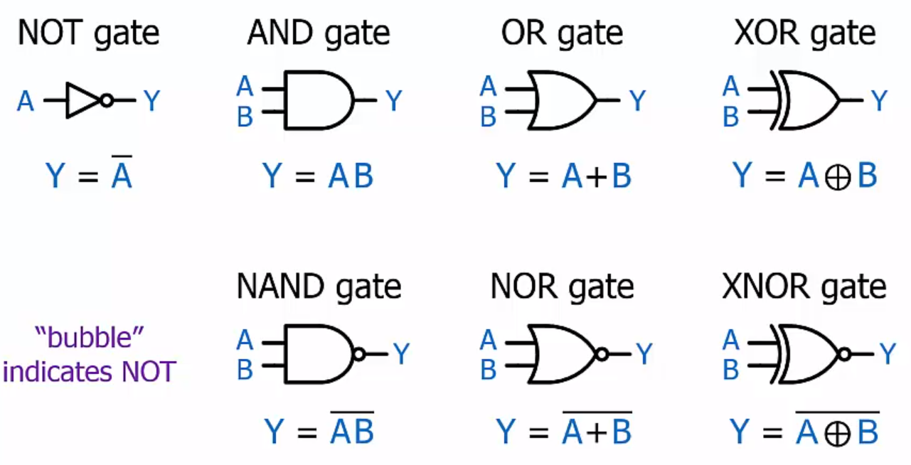
Logic Functions
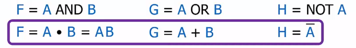
- AND: result is true if all operands are true
- OR: result is true if any operand is true
- NOT: result is the opposite of the operand value
- XOR: the result of a two-operand OR is true if both operands are true, the odd function
- A bitwise operation computes each bit of an N-bit result based on the value in the correponding position of the N-bit operands.
Combiational Logical
- Waveforms: a waveform is a visual way to represent signal values over time.
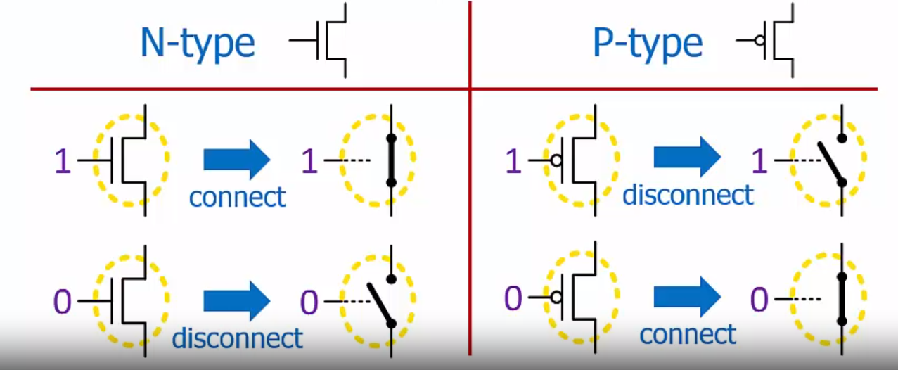
- Logic circuits are at a higher level of abstraction. Each transistor acts like a switch.
- NOT gate use 2 transisters.
Combinational Blocks
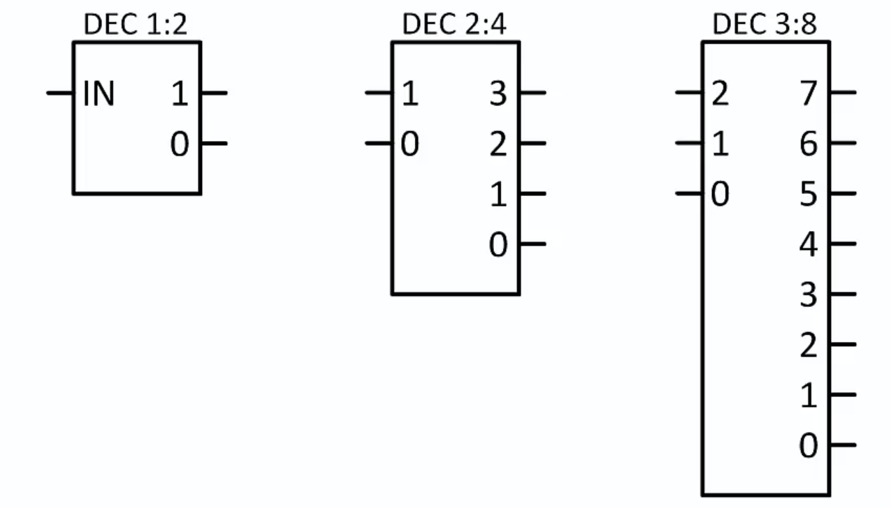
- Decoder: converts an n-bit input code word into a unique m-bit ouput value, where $m=2^n$.
- Exactly one output can be true at any given time.
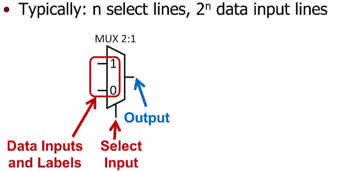
- Multiplexers: based on the select input, choose one of the data inputs to drive the output
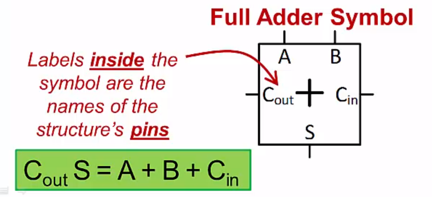
- Full adder: at every position, determine 2-bit sum of adding each addend’s bit in that position plus a carry-in. A full adder performs addition for single bit position.
- Ripple Carry Adder: serires of full adders, where each full adder performs the addition for a single bit position.
Week 5
Sequence Logic
- Before, are all combinational logic. Circuit outputs only depend on current input values.
- A circuit’s current state is the binary number that is currently stored in the circuit’s flip-flops.
- Sequence logic: circuit outputs depend on both current input values and past stored values.
- D flip-flop: output is always equal to the value it is storing
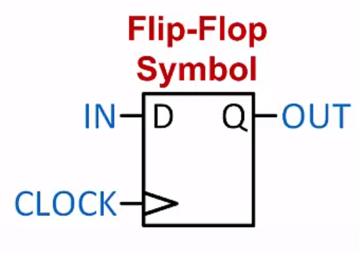
- D flip-flop updates when the clock transitions from 0 to 1 (rising edge)
- FSM (finite state machine): any circuit built from flip-flops is FSM
- State Diagram:
- state is represented by a circle, the circle also indicate the output in that state.
- state transitions represented by an arrow from one state to another. Labeled with the input condition.
FSM
- sequential circuits.
- track of which state it is currently in
- The FSM contains one flip-flop per bit of state
- depends both upon the current state and the inputs, the next state is a function of the current state and current input values.
- Start state <-> reset state
- Some state machines do not have an input, or the input does not affect a particular state transition, this type of transition is an unconditional transition.
- “X” means shorthand for “any value of”
- The output will be the current state output.
Registers Memory
- A register is a group of flip-flops used to stire multi-bit binary values.
- Write-Enable: whether take the input to store
- Address: M bits, $2^M$ locations to access.
- Each location stores a single N-bit word: data size, # bits per location
- Capacity = (# locations) * (data size)
- Address selects which register supplies data out using Mut.
- Address selects which register may be written to using decoder. Selected register will only be written if WE=1
Week 6
- ALU(arithmetic logic unit), a set of logic structures that perform a set of different possible computations on the inputs.
- A set of multiplexers that choose which result to send to the ALU output.
- The register file: a small memory located near the ALU
write port: used to write operation’s result to register file: DR(DA), DD(DD), write
read port: used to get operands from register file: SR(SA), SD, BMUX, output - Conceptual Compute Model: Memory, Control Unit, Processing Unit
- Control Unit: fetches instructions one by one from memory, two special unit PC(program counter), IR(instruction register). Memory read using address in PC, put the returned value into IR, then increment the PC.
- von Neumann Compute Model, holds both the program and any data needed by the program(memory)
- Instruction: small step of a program is encoded into a binary word called an instruction. (ISA)
- FETCH: Read an instruction from mem, put into IR and increase PC
-> DECODE: determine what the instruction meaning (opcode, field)
-> EVALUATE ADDRESS
-> FECTCH OPERANDS: get the operands
-> EXECUTE: ALU
-> STORE RESULT: write back to register
repeat forever, not all phases are required for all instruction(后四个) - Some processors group different stage together
Week 7
- LC-3: 8 general-purpose registers, 16 bit
- N, Z, P: three branch bit reg
- address calculation method depends on the memory addressing mode.
- Mem both holds ins and data
ECE 252
https://harukimoriarty.github.io/2023/09/19/EE252/